Design Inverter Gate by Using Nand Gates
Aim
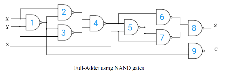
To study and verify the Full Adder using NAND Gates.Learning Objectives
- To understand the behavior and demonstrate Full Adder Using NAND Gates.
- To apply knowledge of the fundamental gates to create truth tables.
- To develop digital circuit building and troubleshooting skills.
- To understand key elements of TTL logic specification or datasheets.
IC Used
| IC Number | IC Name |
|---|---|
| 74LS00 | Quad 2-input NAND Gates |
Circuit Tutorials:
- Full Adder Using NAND Gates
Procedure
- Place the IC on IC Trainer Kit.
- Connect VCC and ground to respective pins of IC Trainer Kit.
- Implement the circuit as shown in the circuit diagram.
- Connect the inputs to the input switches provided in the IC Trainer Kit.
- Connect the outputs to the switches of O/P LEDs
- Apply various combinations of inputs according to the truth table and observe the condition of LEDs.
- Note down the corresponding output readings for various combinations of inputs.
- Power Off Trainer Kit, disconnect all the wire connections and remove IC's from IC-Base.
Theory
HALF ADDER - An adder is a digital logic circuit in electronics that implements the addition of numbers. In many computers and other types of processors, adders are used to calculate addresses, similar operations, and table indices in the ALU and also in other parts of the processors. These can be built for many numerical representations like excess-3 or binary coded decimal. Adders are classified into two types: half adder and full adder. The half adder circuit has two inputs: A and B, which add two input digits and generate a carry and sum.
An adder is a digital circuit that performs the addition of numbers. The half adder adds two binary digits called as augend and addend and produces two outputs as the sum and carry; XOR is applied to both inputs to produce the sum and AND gate is applied to both inputs to produce carry.

By using a half adder, you can design simple addition with the help of logic gates. A half adder is used to add two single-digit binary numbers and results into a two-digit output. It is named as such because putting two half adders together with the use of an OR gate results in a full adder. In other words, it only does half the work of a full adder.
FULL ADDER - This adder is difficult to implement than a half-adder. The difference between a half-adder and a full-adder is that the full-adder has three inputs and two outputs, whereas half adder has only two inputs and two outputs. The first two inputs are A and B and the third input is an input carry as C-IN.
A full adder is a digital circuit that performs addition. Full adders are implemented with logic gates in hardware. A full adder adds three one-bit binary numbers, two operands, and a carry bit. The adder outputs two numbers, a sum and a carry bit.

Then the full adder is a logical circuit that performs an addition operation on three binary digits and just like the half adder, it also generates a carry out to the next addition column. Then a Carry-in is a possible carry from a less significant digit, while a Carry-out represents a carry to a more significant digit.
NAND gate - It is a digital circuit that has two or more inputs and produces an output, which is the inversion of logical AND of all those inputs.
Logic NAND Gates are available using digital circuits to produce the desired logical function and is given a symbol whose shape is that of a standard AND gate with a circle, sometimes called an "inversion bubble" at its output to represent the NOT gate symbol with the logical operation of the NAND gate.
As with the AND function seen previously, the NAND function can also have any number of individual inputs and commercial available NAND Gate IC's are available in standard 2, 3, or 4 input types. If additional inputs are required, then the standard NAND gates can be cascaded together to provide more inputs.
Boolean Expression Y = (A.B)'
"If either A or B are NOT true, then Y is true"

NAND gate operation is same as that of AND gate followed by an inverter. That's why the NAND gate symbol is represented like that.
Block Diagram
Precautions
- Make the connections according to the IC pin diagram.
- The connections should be tight on trainer kit.
- The Vcc and ground should be applied carefully at the specified pin only.
Conclusion
We have learned the Full Adder Using NAND Gates.Recommendations
-
Half Adder Using Basic Gates
Aim: To study and verify the Half Adder Using Basic Gates.
ICs used: 74LS86 74LS08 -
Full Subtractor using Two half adders basic gates
Aim: To study and Verify the Full Subtractor using Two half adders basic gates.
ICs used: 74LS86 74LS04 74LS08 74LS32 -
Half subtractor using basic gates
Aim: To study and Verify the Half subtractor using basic gates.
ICs used: 74LS86 74LS04 74LS08 -
Half Adder using NAND Gates
Aim: To study and verify the Half Adder using NAND Gates.
ICs used: 74LS00 -
Full Adder function using 3:8 Decoder
Aim: To study and Verify the Full Adder function using 3:8 Decoder.
ICs used: 74LS138 74LS20
Design Inverter Gate by Using Nand Gates
Source: https://www.deldsim.com/study/material/12/full-adder-using-nand-gates/
Belum ada Komentar untuk "Design Inverter Gate by Using Nand Gates"
Posting Komentar